Front end data acquisition (DAQ) systems are first thing a physics interaction sees when encountering an experiment. The electronic components on different experiments come in varying forms, however, all DAQ systems share a common theme: Signal processing. Acquiring electrical signals, energy and timing measurements, signal-to-noise optimization, event rates, are some functions a DAQ is tasked with. To highlight some common features of the front end readout system of a detector, consider the figure below:
Incident radiation is collected by a sensor, converting the energy of a particle or a photon into an electrical signal. This signal generally comes in the form of a pulse. The signals collected are usually quite weak and is passed through a preamplifier to boost the signal with a high input impedance and a low output impedance, such that the signal-to-noise ratio (SNR) is preserved.
The signal then makes it way through the main amplifier. Much like the preamplifier, the fidelity of the signal information is kept intact. While the main amplifier’s duty is in the name, it serves another purpose. That is to shape the pulse into a form that can be used for further processing. In pulse shaping, the bandwidth of the system is controlled to improve the SNR, and by extension, setting the overall noise contribution of the system, also limiting the maximum signal rate.
Finally, this low level analog pulse fed into an Analog-to-Digital Converter (ADC), quantizing the signal. In other words, sampling continuous or varying signals into discrete packets in the form of a bit pattern. Once converted into a discrete-amplitude digital signal, the signal is set for storage, further processing, and eventually, data analysis.
This section should provide a quick summary of common units throughout the signal processing chain.
As stated before, ADCs samples continuous waveforms into discrete bit logic patterns that are unique to the input information. A simple ADC design is shown in Figure [pf].
[adc.png]
Through a series of voltage dividers, the input signal travels through a several comparators (a gate that compares voltages) with increasing threshold conditions. The encoder translates the output pattern of the comparators to provide a binary interpretation of the input signal.
Discriminators are devices or circuits that trigger an output logic pulse when a certain threshold is reached. For the purposes of signal processing, discriminators fall into a few categories (see section on Timing Techniques), however, their common purpose is to decide if the input is interesting.
In the case of particle interactions or measurements, where events are few and far between (such as time-of-flight and lifetime measurements), Time-to-Digital Converters (TDC) are used to timestamp pulse data through some form of counter or clock.
The simplest form of a TDC involves a counter that enumerates clock pulses with a start and stop signal. However, counters fall short on resolution (\(\approx\) 1 ns) due to limitations on clock frequency \cite{spieler}.
High resolution digitization can be done using analog techniques, also known as ramp interpolation. Using a current source, \(I_{T}\), time intervals are translated into voltages via a capacitor. Mathematically,
\[V = \frac{I_{T} (t_{stop} - t_{start})}{C}\]Compared to the counter technique, ramp interpolation resolution is on the order of picoseconds.
Aptly named, amplifiers increase the power of an incident time varying signal. There are three three different basic types of amplifiers, or rather, amplifiers can operate in different mode based on the ratio of input resistance and source resistance.The time response of will affect the measured pulse shape, as a result, all amplifiers contribute to the pulse shape.
The input signal voltage for voltage sensitive amplifiers is
\[V_{i} = \frac{R_{i}}{R_{s} + R_{i}}V_{s}.\]Input resistance \(R_{i}\) needs to much larger than the source impedance. When acting as an integrator, the capacitance of the detector and any input capacitance must be summed over (see section on Integrating Circuits).
Current sensitive amplifiers are another mode of amplifier operation and and are commonly used in timing applications, where the signal is fed into a discriminator. The input current \(i_{s}\) is given by
\[i_{i} = \frac{R_{s}}{R_{s} + R_{i} i_{s}}.\]Inverting the conditions for a voltage sensitive configuration, the input resistance needs to be much smaller than the source impedance.
Last but not least are charge sensitive amplifiers which integrates charge on a feedback capacitor and can be used to control gain and input resistances. These find uses in energy spectroscopy where charge and time of an event is of interest.
An alternative and more efficient method of dealing with amplitude variations is constant fraction triggering. The idea is to find the maximum of the pulse using the point at which the slope is \(0\). The pulse is divided into the components, delay time (\(t_{d}\)) and rise time (\(t_{r}\)) and a comparator is used to determine which voltage is let through.
Consider a pulse with linear leading edge with conditions regarding the rise time \(t_{r}\). For \(t \leq t_{r}\),
\begin{equation}
V(t) = \frac{t}{t_{r}},
\end{equation}
The signal at the comparator input is
\begin{equation} V(t) = \frac{t-t_{d}}{t_{r}} V_{0} \end{equation}
It can be shown that when the signal crosses the threshold \(t>t_{r}\), where \(V(t) = V_{0}\), the time at which the comparator gives an output signal is
\begin{equation} t = f_{a} t_{r} + t_{d} \end{equation}
provided that \(t_{d} > t_{r}\). From here the constant fraction \(f_{a}\) independent of the peak amplitude is obtained. Note that \(f_{a}\) is the attenuation factor of a the input signal, \(\textit{not}\) a frequency.
Moreover, reducing the delay time such that \(t_{d} < (1-f_{a}) t_{r}\), produces an equation that is independent of both the amplitude and rise time,
\begin{equation} t = \frac{t_{d}}{1-f} \end{equation}
where \(t_{d} = t_{r} (1-f_{a})\). Relating this back to the trigger voltage, the maximum threshold signal \(V_{T} = f_{a} V_{0}\) In other words, signal that passes through and attenuated by the factor \(f_{a}\) of the original amplitude.
Simply put, constant fraction discriminators elimate timing jitter. An incoming pulse is split into two pulses \(A\) and \(B\). Suppose there are resistances in the two wires, making pulse \(A\) larger than pulse \(B\). Pulse \(A\)’s wire is extended so that it lags behind pulse \(B\), meanwhile, pulse \(B\) is inverted, giving a positive pulse. When these two pulses are added together, a bipolar pulse is created such that there is a zero crossing. This zero crossing point is independent of the pulse amplitude and (timing jitter)?
The Nuclear Instrumentation Module (NIM) standard refers to the set of application specific electronic modules (Figure \ref{nimmodules}) that sit in standardized bins (Figure \ref{nimbin}). Each of these modules can be purposed with implementing basic logic operations, take the role of an amplifier or discriminator, and any of the other signal processing components. The back of each module are standardized by the Department of Energy \cite{wikipedia_2021}. The advantage is in the idea a modular system where electronic instrumentation can be interchange for rapid prototyping or updating the electronic design.
When a particle or a photon reaches the detector, the first order of business is to determine the energy deposited, which is directly related to the pulse amplitude. The equation below describes how the absorbed energy \(E\) is related to the detector signal current.
\(E \propto Q_{s} = \int^{T_c}_{0} i_{s} (t) dt\),
where \(E\) is the deposited energy and \(Q_{s}\) is the total charge. The signal usually comes in the form of a short current pulse \(i_{s}\) which can be integrated over the time it takes for the signal to reach the detector electrodes, denoted \(T_c\). Then the signal needs to couple from the sensor to the amplifier, in most cases, using a preamplifier to boost a weak input signal. At this point, the signal has seen some level of pulse shaping since it passes through amplifiers and CR-RC filters.
The objective of signal processing is two-fold, and are in conflict with each other. In order to decrease pileup in high count rate experiments and improve pulse pair resolution, the pulse width is decreased to reduce distortions caused by amplitude overlap. On the other hand, there is the persistent aim in improving the SNR, which calls for the broadening of a narrow current pulse. So, the optimization between these goals in pulse shape design are determined based on the application.
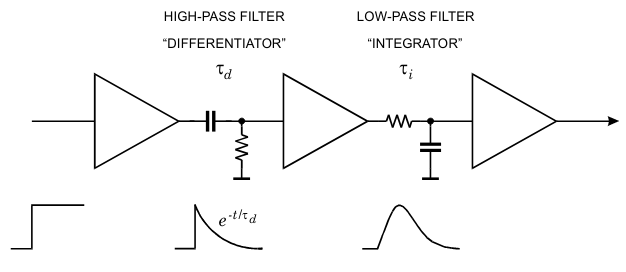
To explore this balance of objectives, consider a simple arrangement of CR-RC shapers shown in Figure \ref{crrc} and \ref{chain}(see appendix for details on RC and CR circuits) which contain the essential pulse shaping conventions.
The use of \(CR\) and \(RC\) high/low pass filters set the frequency constraints for a some time constant \(\tau\). Adjusting the upper frequency bound sets the rise time. Lower frequency bounds sets the duration of the pulse.
A quick aside on Fourier transforms, a convolution is defined in terms of an integral transform as
\[f(t) * g(t) \equiv \int_{-\infty}^{\infty} f(\tau) g(t-\tau) d\tau\]As it relates to a CR-RC shaper, the output pulse is a convolution of the input signal (or current from the sensor) \(V_{i}(t)\) and the impulse response \(g(t)\). For a CR-RC chain like the one shown in Figure \ref{chain}, the output pulse shape can be written as
\[V_{0} (t) = V_{i} (t) * g_{int} (t) * g_{diff} (t)\]For equal CR and RC circuits filers with equal time constants, the assumption that the output pulse has a max peak at time \(\tau = \tau_{RC} = \tau_{CR}\), \(V_{0}\) can be approximated to
\[V_{0} = \frac{t}{\tau} e^{-t/\tau}\]Seeing that SNR is mentioned throughout this paper, optimization of this ratio should be considered at every stage of DAQ which can be used to characterize the efficiency of electrical components. In the context of conventional theory, the SNR is typically defined in terms of \(\textit{average power}\)
\[\frac{S}{N} = \frac{P_{signal}}{P_{noise}}\]Sometimes it may be more useful to define the SNR using the voltage Root Mean Square (RMS) for time varying functions. Recall the familiar power-voltage equation \(P = V^{2}_{rms}/R\). In signal processing, the standard is to take \(R=1\Omega\), leaving the SNR in terms of \(V_{rms}\)
\begin{equation} \frac{S}{N} = \bigg(\frac{A_{S}}{A_{N}}\bigg)^{2} \end{equation}
where \(A_S\) and \(A_N\) are the amplitudes of the signal and noise RMS voltages respectively.
When examining systems that measure signal charge, such as an amplifier, recall that the voltage magnitude is inversely proportional to the sum of the detector capacitance (\(C_d\)), amplifier input capacitance (\(C_{i}\)). That is, the SNR is inversely proportional to the total capacitance \(C\) at input,
\begin{equation} \frac{S}{N} \propto \frac{1}{C}. \end{equation}
However, note that as \(C\rightarrow 0\), the electronics are switched to current mode.
Since optimization of the SNR is important, some exposition on types of noises and their sources will be helpful when designing and troubleshooting signal processing.
The most common type of noise are caused by thermal agitations of electrons in a resistor, otherwise known as Johnson-Nyquist noise.
The connection between noise sources and temperature \(T\) can written in many ways. The following equation is the thermal noise power density
\begin{equation} \frac{dP_{noise}}{df} = 4k_{b}T. \end{equation}
This derivative is the power per unit bandwidth or \(\textit{spectral density}\) and \(k_{b}\) is the Boltzmann constant.
Also, since \({dP_{noise}}/{df}\) is a constant, thermal noise by definition, is a form of white noise. More spectral density equations can be derived in terms of the electronic variables via the use of \(P = \frac{V^{2}}{R} = I^{2} R\). The importance of this equation is to show that the total noise depends on the bandwidth of the system.
Another type of noise is cause by random fluctuations of flowing charge carriers. Based on Poissonian statistics for electron flow, shot noise be described as the current spectral density at some frequency \(\omega\)
\begin{equation} I_{noise}^{2} = 2 e I \end{equation}
where \(e\) is the electron charge and \(I\) is the average current. Note that the equation describes the flow of \(\textit{discrete}\) electrons, so shot noise is typically not an issue. However, the effects of shot noise begin to take weight at wider bandwidths. Shot noise is also example of white noise since the spectral density is frequency independent.
A common source of noise is low frequency pink noise and is ubiquitous in nature, from astronomical phenomenon to biological systems. In the context of electronics and condensed matter, slow fluctuations of defects and trapping in metals, dielectrics, and semiconductors contribute to a \(1/f\) spectrum. Also named “\(1/f\)” noise, it is defined as the total noise between frequency bands \(f_{1}\) to \(f_{2}\) over the inverse frequency distribution
\[V^{2}_{noise} = \int_{f_{1}}^{f_{2}} \frac{A_{f}}{f} df = A_{f} \log \frac{f_{2}}{f_{1}}\]where the voltage spectral density is \(A_{f}/f\). \(f_{2}/f_{1}\) shows that the total noise is dependent on the ratio of upper to lower cutoff frequencies.
So far the discussion has been about optimizing the SNR. However, the methods and techniques in timing measurements on the scale of elementary particle lifetimes takes a slightly different approach. Timing fluctuations are introduced throughout the detection process, as a result of noise and statistical fluctuations. Many of these approaches can be condensed into “slope-to-noise” techniques.
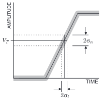
One of the first encounters with time-interval fluctuations is an effect called jitter, producing a “spread” in the time signal. To mitigate this, the technique of Leading Edge (LE) triggering is employed. In Figure \ref{letrigger1}, the timing variance \(\sigma_{t}\) for a fixed amplitude is expressed as,
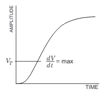
\[\sigma_{t} = \frac{\sigma_{n}}{\|\frac{dV}{dt}\|}\]where \(\sigma_{n}\) is the noise variance. Seeing that the time variance is inversely proportional to the slope, the trigger level is chosen such at maximum rise time \(dV/dt\) as shown in Figure \ref{letrigger2}.
Another effect to account for are time signal shifts causing a broadening of signal curve which is dependent on the pulse amplitude. This phenomenon is known is “walk”. The technique of fast zero-crossing is employed to mitigate this.

To show this, consider a CR-RC shaper with equal time constants \(\tau\), normalized as \(T \equiv t/\tau\). The bipolar output voltage is
\begin{equation} V_{b}(T) \equiv \frac{dV_{t}(T)}{dt} = V_{0} e^{-T} (1-T) \end{equation}
where \(V_{u} (T) = V_{0} T e^{-T}\) has been formed into a bipolar output signal by a differentiator (double delay line shaping). At \(T=1\) or when \(t=\tau\), zero crossing occurs and the trigger is set at.
An alternative and more efficient method of dealing with amplitude variations is constant fraction triggering. The idea is to find the maximum of the pulse using the point at which the slope is \(0\). The pulse is divided into the components, delay time (\(t_{d}\)) and rise time (\(t_{r}\)) and a comparator is used to determine which voltage is let through.
Consider a pulse with linear leading edge with conditions regarding the rise time \(t_r\). For \(t \leq t_{r}\),
\begin{equation}
V(t) = \frac{t}{t_{r}},
\end{equation}
The signal at the comparator input is
\begin{equation} V(t) = \frac{t-t_{d}}{t_{r}} V_{0} \end{equation}
It can be shown that when the signal crosses the threshold \(t>t_{r}\), where \(V(t) = V_{0}\), the time at which the comparator gives an output signal is
\begin{equation} t = f_{a} t_{r} + t_{d} \end{equation}
provided that \(t_{d} > t_{r}\). From here the constant fraction \(f_{a}\) independent of the peak amplitude is obtained. Note that \(f_{a}\) is the attenuation factor of a the input signal, \(\textit{not}\) a frequency.
Moreover, reducing the delay time such that \(t_{d} < (1-f_{a}) t_{r}\), produces an equation that is independent of both the amplitude and rise time,
\[t = \frac{t_{d}}{1-f}\]where \(t_{d} = t_{r} (1-f_{a})\). Relating this back to the trigger voltage, the maximum threshold signal \(V_{T} = f_{a} V_{0}\) In other words, signal that passes through and attenuated by the factor \(f_{a}\) of the original amplitude.
Before processing a signal, it is important to introduce some terminology that characterizes a pulse signal. Suppose we have an square pulse as shown in the figure below.
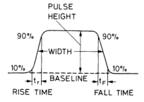
Beginning with the baseline, this is the “null” or “ground state” of the pulse. In the figure it is shown as zero, but this can vary due to pulse shape or count rate. The pulse height is taken as the instantaneous maximum of the pulse signal, measured from the baseline. The pulse width is measured as the full width half max (FWHM), which defines the bandwidth of the signal. The leading and falling edge corresponds to the section of the pulse seen at \(t_0\) and when the full pulse as passed, respectively. The rise time (\(t_r\)) refers to the section the signal rises from \(10\%\) to \(90\%\) of the max amplitude. Similarly, fall time is the section of the pulse that drops from \(90\%\) to \(10\%\) of the pulse height. Pulse signals can also be categorized into unipolar or bipolar. The former describes a pulse that occurs on one side of the baseline and the latter describes a signal that continues onto the other side of the baseline.
In a preceding discussion, integration amplifiers and ADCs are mentioned as commonly used option for efficient signal detection. Another straight forward method is to consider the sensor capacitance. At the heart of these techniques is an $RC$ circuit, which is the electrical counterpart of an integration.
\[V_{out} \approx \frac{1}{\tau}\int V_{in} dt\]where \(\tau = RC\) is the characteristic output time constant, which also determines the cutoff or corner frequency,
\[f \geq \frac{1}{2\pi \tau}\]It can be shown that for small values of \(\tau\), the integral reduces to \(V_{in} \approx V_{out}\). \(\tau\) can be rewritten as
\[\tau = R (C_{d}+C_{i})\]where \(R\) is the input resistance, \(C_d\) is the induced charge capacitance (charge buildup on sensor electrodes), and \(C_i\) is the input capacitance which is intrinsic to the amplifier.
For time constants that are much larger than the pulse duration, the amplifier input voltage can be written as
\[V_{i} = \frac{Q_s}{C_d + C_i}\]showing that the signal magnitude is a function of the sensor capacitance.
In other words, the \(RC\) circuit also is part of the pulse shaping process. At \(\tau >> V_{in}\), the circuit acts as a high frequency filter contributing to the pulse shape by removing noise from the signal.
Accompanying the low pass filter integrator circuit, the \(CR\) circuit performs a differentiation on a pulse input voltage,
\[\frac{dV_{in}}{dt} \approx \frac{1}{\tau} V_{out}\]and of course, the expression low frequency filters is reversed,
\[f \leq \frac{1}{2\pi\tau}\]The differentiation is carried out if the time constant is much larger than the width of the pulse.
For reference, here a truth table containing bitwise operations for AND, OR, NAND, NOR, XOR, Conditionals,and Biconditionals.
\[\begin{array}[] \hline P & Q & AND & OR & NAND & NOR & XOR & Conditional & Biconditional \\ \hline 1 & 1 & 1 & 1 & 0 & 0 & 0 & & \\ \hline 1 & 0 & 0 & 1 & 1 & 0 & 1 & & \\ \hline 0 & 1 & 0 & 1 & 1 & 0 & 1 & & \\ \hline 0 & 0 & 0 & 0 & 1 & 1 & 0 & & \\ \hline \end{array}\]Given \(P\) and \(Q\) inputs, the outputs are as follows:
In order to indicate to the compiler to evaluate a binary number, the number prefixed with \(0b\). For instance, the number \(10\) in 8-bit binary can be written as:
\[0b00001010\]One can “flip” a bit by applying/masking the binary with another by referring to the truth table above. For instance an AND operation on an 8-bit binary would look like:
\(0b00001010\) AND \(0b00000010\) = \(0b00000010\)
An OR operation:
\(0b00001010\) OR \(0b00000100\) = \(0b00001110\)
The NOT operator, usually denoted by a ~ preceeding the binary number, can be applied to flip each bit to its opposite value:
\[0b1010\] \[\tilde{}0b0101\]Bit-wise operations will be used to control registers on a chip. Depending on the chip type, each register will be displayed as a number of bits that can be changed by applying a mask of the same number of bits to control the features of a chip. Below are examples of setting clearing a bit in a register.