A mix of topics related to solid state physics and materials science.
\(\let\vec\mathbf\) \(\newcommand{\v}{\vec}\) \(\newcommand{\d}{\dot{}}\) \(\newcommand{\abs}{\rvert}\) \(\newcommand{\h}{\hat}\) \(\newcommand{\f}{\frac}\) \(\newcommand{\~}{\widetilde}\) \(\newcommand{\<}{\langle}\) \(\newcommand{\>}{\rangle}\)
A lattice is just an infinite array of points equally spaced such that the likeness of the (crystal) structure is preserved when viewed from a different lattice point.
Lattice positons in a crystal can be represented as a linear combination. For an arbitrary lattice position, \(\v{t}\):
\[\v{t} = u \v{a} + v \v{b} + w \v{c}\]Alternatively, for a so-called Bravais Lattice, a set of points in space generated by a linear combination of lattice vectors:
\[\v{R} = u_{1} \v{a} + u_{2} \v{b} + u_{3} \v{c}\]where \(\v{a}\), \(\v{b}\), \(\v{c}\) are linearly independent vectors (i.e. they do not lie in the same plane).
In summary, a crystal structure is:
\[{Crystal Structure} = {Bravais Lattice} + {Basis}\]Lattice planes can be described using the set of points that intersect the axes:
\[a/h , b/k , c/l\]where \(h,k,l\) are integers and are known as Miller Indicies. For instance, a plane can be denoted as \((hkl)\).
The atomic packing factor is the defined as:
\[\frac{ V_{atoms} }{ V_{cell} }\]Where \(V_{atoms}\) represents the volume occupied by atoms of radius \(R\) and \(V_{cell}\) is the volume occupied by the unit cell, usually occupying a volume of \(a^{3}\) (\(a\) being the distance across an edge).
The FCC unit cell has a total of 4 atoms within. Assuming each atom occupies a spherical volume:
\[V_{atoms} = 4 \cdot \frac{4}{3} \pi R^{3} = \frac{16}{3} \pi R^{3}\]For a FCC unit cell, the atoms across the face of a unit cell have a distance of \(4R\). The diagonal across a face is then:
\[a^{2} + a^{2} = (4R)^{2}\]Solving for \(a\):
\[a = 2R\sqrt{2}\]So the total volume of the unit cell is:
\[V_{cell} = a^{3} = (2R\sqrt{2})^{3} = 16R^{3}\sqrt{2}\]All together the APF of an FCC unit cell is:
\[APF = 0.74\]In a similar fashion, the BCC unit cell contains two atoms:
\[V_{atoms} = 2 \cdot \frac{4\pi R^{3}}{3} = \frac{8 \pi R^{3}}{3}\]However, the “\(4R\) diagonal” goes across the center of the BCC cell. After a couple applications of the pythagorean theorem, the \(4R\) diagonal is:
\[c = \sqrt{3} a = 4 R\]Now finding the volume of the unit cell,
\[a^{3} = \bigg( \frac{4R^{3}}{\sqrt{3}} \bigg)\]Putting it all together, the BCC atomic packing factor is,
\[\frac{V_{atoms}}{V_{cell}} = \frac{9\pi}{8 \sqrt{3}^{3}} = 0.68\]For a given crystal structure, incident x-rays produce characteristic patterns due to constructive interference by the so called Bragg Condition:
\[n \lambda = 2 d sin \theta\]X-rays of wavelength \(\lambda\) are scattered by crystal planes and constructively interfer such that the path difference is an interger number, \(n\), of wavelengths depending on the angle \(\theta\) of the incident wave.
Using X-ray diffraction and electron microscopy atoms, we know that electrons are arranged uniformly in a lattice due to a periodic potential. In a one dimensional model, there are two models to consider:
For now, we use the Kronig-Penny model to determine the behavior of an electron in a periodic potential. Starting from the Schrodinger equation:
\[- \frac{\hbar}{2m} \frac{d^{2} \psi}{d x^{2}} + V(x) = E \psi\]As stated before, we solve the equation for two regions, \(I\) and \(II\).
In region \(I\), the potential is \(V(x) = 0\):
\[\frac{d^{2} \psi}{d x^{2}} + \frac{2m}{\hbar^{2}} E \psi = 0\]The solved energy comes out to be:
\[\frac{2m}{\hbar^{2}} E = \alpha^{2} \rightarrow E = \frac{\hbar^{2}}{2m} \alpha^{2}\]In region \(II\), \(V(x) = V_{0}\):
\[\frac{d^{2} \psi}{d x^{2}} + \frac{2m}{\hbar^{2}} (E - V_{0}) \psi = 0\]Let \(\gamma^{2} = \frac{2m}{\hbar^{2}} (V_{0} - E)\)
To solve for these to regions simultaneously, we use the Bloch Function:
\[\psi(x) = U(x) e^{ikx}\]where \(U(x)\) is a periodic potential. Product differentiation to the second order gives:
\[\frac{d \psi}{d x} = \frac{d U(x)}{dx} e^{ikx} + U(x) ik e^{ikx}\] \[\frac{d^{2} \psi}{d x^{2}} = i \frac{d U(x)}{d x} e^{ikx} + \frac{d^{2} U(x)}{dx} e^{ikx} + i \frac{d U(x)}{dx} e^{ikx} + i^{2} k^{2} U(x) e^{ikx}\] \[= e^{ikx} \bigg[ \frac{d^{2} U(x)}{dx^{2}} + 2 i k \frac{d U(x)}{dx} - k^{2} U(x) \bigg]\]Now its just a matter of plugging in the solved quantities into the differential equations. In region \(I\):
\[\frac{d^{2} U(x)}{dx^{2}} + 2ik \frac{d U(x)}{dx} - (k^{2} - \alpha^{2}) U(x) = 0\]In region \(II\):
\[\frac{d^{2} U(x)}{dx^{2}} + 2ik \frac{d U(x)}{dx} - (k^{2} + \alpha^{2}) U(x) = 0\]We arrive at the master equation:
\[\frac{d^{2} U(x)}{dx^{2}} + D \frac{d U(x)}{dx} + C U(x) = 0\]The general solution to this equation is:
\[U(x) = e^{- \frac{D}{2} x} \bigg[ Ae^{i \eta x} + Be^{-i \eta x} \bigg]\]where \(\eta = \sqrt{ C - \frac{D^{2}}{4}}\)
The solutions for regions \(I\) and \(II\) are as follows:
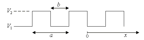
From here, determine coefficients \(A, B, C, D\) from boundary conditions (refer to V(x) graph).
Boundary Condition \(1\): The first boundary condition is at \(x = 0\), the wave function of both regions must be equal to each other:
\[\Psi_{I} = \Psi_{II}\]which implies:
\[A + B = C + D\]Boundary Condition \(2\): The wavefunctions must also be continuous through their derivatives at \(x=0\):
\[\frac{d}{dx} \Psi_{I} = \frac{d}{dx} \Psi_{II}\] \[\bigg( \frac{d U(x)}{dx} \bigg)_{I} = \bigg( \frac{d U(x)}{dx} \bigg)_{II}\]Again we solve for regions \(I\) and \(II\) evaluating the derivatives at \(x = 0\) :
Region \(I\):
\[\frac{d U(x)}{dx} = - i k A e^{i \alpha x} + A i \alpha e^{-ikx} - i k B e^{i\alpha x} + B (- i \alpha) e^{i k x}\] \[\frac{d U(x)}{dx}\bigg|_{x=0} = -ik A + A i \alpha - ik B + B (-i \alpha)\] \[= A ( i\alpha - ik) - B ( i \alpha + ik)\]Region \(II\):
\[\frac{d U(x)}{dx} \bigg|_{x=0} = C (-\gamma - ik ) + D (\gamma - ik)\]Therefore, the derivatives at \(x = 0\) can be written as:
\(A (i \alpha - ik) - B (i \alpha + ik) = C (-\gamma - ik) - D (\gamma - ik)\) Boundary Condition \(III\):
\[\Psi_{I} (x=a) = \Psi_{II} (x=-b)\]and
\[U_{I} (x=a) = U_{II} (x=-b)\]The resulting evaluation:
\[A e^{(i \alpha - ik) a} + B e^{(i \alpha - i k) a } = C e^{(ik + \gamma)b} + D e^{(ik - \gamma) b}\]Boundary Condition \(4\):
As before, the wavefunctions must be continuous through its derivatives:
\[\frac{d U(x)}{dx} \bigg|_{I (x=a)} = \ \frac{d U(x)}{dx} \bigg|_{II (x=-b)}\]The result:
\[A i (\alpha - k) e^{i\alpha(a-k)} - Bi(\alpha+k) e^{i\alpha(a+k)} = -C (\gamma + ik) e^{(ik+\gamma)b} + D(y-ik) e^{(ik - \gamma)b}\]Most of this will be “left as an exercise to the reader”, but I will at least leave some bread crumbs along the way:
Making use of Euler’s equations:
\[e^{ix} = \cos(x) + i \sin(x)\] \[\cos(x) = \frac{1}{2} (e^{ix} + e^{-ix})\] \[\sin(x) = \frac{1}{2i} (e^{ix} - e^{-ix})\]we arrive at:
\[\frac{\gamma^{2} - \alpha^{2}}{2\alpha\gamma} \sinh(\gamma b) \sin(\alpha a) + \cosh(\gamma b) \cos(\alpha a) = \cos(k (a+b))\]Using the following approximations and definitions:
We can simply \(\gamma\) which also extends to \(\gamma b\):
\[\gamma = \sqrt{ \frac{2m}{\hbar^{2} } (V_{0} - E)} \approx \sqrt{\frac{2m}{\hbar^{2}} V_{0}}\]For small \(\gamma b\):
\[\cosh(\gamma b) \approx 1\] \[\sinh(\gamma b) \approx \gamma b\]These approximation simplify the periodic solution to:
\[\frac{P \sin(\alpha a)}{\alpha a} + \cos(\alpha a) = \cos(k a)\]There are two important expressions to be aware of when identifying regions of Bloch-like solutions, namely:
\[P = \frac{ m V_{0} b a}{\hbar^{2}}\] \[\alpha = \frac{\sqrt{2mE}}{\hbar}\]\(P\) is known as the Penny constant, which determines the size of the allowed solutions in a periodic potential. Similarly, \(\alpha\), which is proportional to \(E\) determines the variation of the forbidden bands. i
Given that \(a\) is the separation distance between atoms in a lattice, below is a plot of the allowed solutions to the Schrodinger equation.
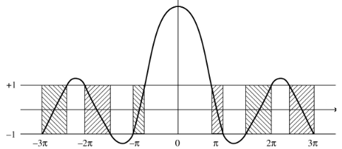
Notice that allowed energy solutions are represented by the shaded regions, for any value of \(\alpha a = \frac{\sqrt{2mE}}{\hbar} a\) that lies between \(\pm 1\).
From here, some cases can be applied to investigate the behavior of the system.
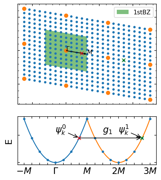
As a result of solving the Schrodinger equation in a periodic lattice, i.e. Bloch’s theorem, the wavevectors \(k\), will provide an infinite number of solutions to the Schrodinger equation. Due to the periodicity of an electron in a crystal system, one can represent all possible wavefunctions by a \(k\) wavevector that simply differs by a reciprocal lattice. This leads to the interpretation of the first Brillouin zone.
The band diagram representation of a Brillouin zone is shown below:
The first Brillouin zone is constructed by as the set of points in \(k\)-space from the origin up to the boundary were the Bragg plane exists, the plane of diffraction in the reciprocal lattice (geometrically, the Bragg plane bisects the reciprocal lattice vectors).
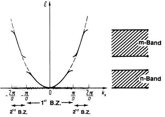
The \(E(k)\) curve can be segmented into regions called Brillouin Zones.
For the case of a one dimensional lattice, the first Brillouin zone exists from \(- \frac{\pi}{a} \leq k \leq \frac{\pi}{a}\). This region is also known as the n-band.
The second Brillouin zone exists from \(- \frac{2\pi}{a} \leq k \leq -\frac{\pi}{a} \cup \frac{\pi}{a} \leq k \leq \frac{2\pi}{a}\), or the m-band.
Consider a monovalent metal such as Sodium which has a bcc strucutre. We assume an electron cloud where each atom contributes one electron to. The number of atoms per cubic centimeter, \(N_{a}\) is given by,
\[N_{a} = \frac{N_{0} \rho}{M}\]where \(N_{0}\) is Avagadro’s number, \(\rho\) is the density of the element, and \(M\) is the mass of the element.
Under the influence of an applied electric field \(\vec{E}\), the electrons experience a force \(e\vec{E}\) and are accelerated towards the anode with a drift described by,
\[m \frac{dv}{dt} = e \vec{E}\]where \(e\) is the charge, \(\vec{E}\) is the applied field, and \(m\) is the electron mass. However, this suggests that as long as the electric field is present, the electrons drift with constant acceleration, which also means that when \(\vec{E}\) is removed, the electrons drift with a constant velocity. Barring a few superconducting materials, this is an unphysical phenomenon.
Materials have an intrinsic resistance that counteracts the electrostatic force \(e \vec{E}\). As electrons move through a material medium, they lose energy due collisions against lattice atoms. Moreover, resistance is dependent on defect properties such as impurities, vacancies, grain boundaries, dislocations, amongst other defect types.
To rectify this, a “friction” term, \(\gamma v\) is added to adjust for electrical resistance.
\[m \frac{dv}{dt} + \gamma v = e \vec{E}\]where \(\gamma\) is a constant and \(v\) is the damping force which also contains the drift velocity.
We consider the steady state case \(v=v_{f}\) where the friction force and the electrostatic force are equal in magnitude, then \(dv/dt = 0\).
\[\gamma v_{f} = e \vec{E}\]Solving for \(\gamma\),
\[\gamma = \frac{e \vec{E}}{v_{f}}\]Reinserting into the adjusted drift velocity equations yields a differential equation for electrons under the effects of an electrostatic force and a resistive force.
\[m \frac{dv}{dt} + \frac{e \vec{E}}{v_{f}} v = e \vec{E}\]The solution for \(v\) is,
\[v = v_{f} \bigg[ 1 - \exp \bigg( - \bigg( \frac{e\vec{E}}{m v_{f}} t \bigg) \bigg) \bigg]\]The average time between collisions or relaxation time is contained within a time constant, \(\tau\),
\[\tau = \frac{m v_{f}}{e \vec{E}}\]This equation can be rearranged to obtain and expression for the final drift velocity \(v_{f}\),
\[v_{f} = \frac{\tau e \vec{E}}{m}\]A quick analysis of units reveals the definition for the mean free path,
\[l = v \tau\]Recall the current density, \(j\):
\[j = N v e\]where \(N\) is the number of electrons per unit volume, \(v\) is the electron velocity, and \(e\) is the charge. The current density, \(j\) can also be written in terms of conductivity, \(\sigma\), and the electric field,
\[j = \sigma \vec{E}\]All together, by combining the two definitions of current density, we can obtain an important expression for conductivity,
\[j = N v e = \sigma \vec{E}\] \[\sigma = \frac{N e^{2} \tau}{m}\]This equation for conductivity, which is now written in terms of the number of free electrons, \(N\), and relaxation time, \(\tau\), reveals that the conductivity is proportional to both variables.
There are a few ways to describe electron mobility, all of these decribe how an electron moves through a medium:
Hole mobility: When electrons make the jump to say, the conduction band, a hole is left behind. Neighboring electrons are attracted and fill the empty spot. The hole appears in a new location, giving it a sense of “mobility”.
Carrier mobility: This term refers to both electron and hole mobility.
Electron mobility can be defined in terms of drift velocity:
\[v_{d} = -\mu_{e} E\]where \(\mu_{e}\) is the electron mobility, \(v_{d}\) is the drift velocity, and \(E\) is the magnitude of the electric field applied across the material. Hole mobility is similary defined:
\[v_{d} = \mu_{h} E\]It is also useful to describe conductivity as it is proportional to the product of mobility and carrier concentration. Usually denoted \(\sigma\), conductivity can be expressed in terms of mobility as:
\[\sigma = N \mu e\]In the presense of impurities or dopants, the path that an electron takes though an impure lattice increases the propability of scattering due to varying disordered potentials. As a result, this affects the total mobility of an electron, which in turn also affects the resistivity. Fortunately, these effects add linearly and are nicely summarized as Matthiessen’s Rule. In terms of the total number of scattering events,
\[\frac{1}{\tau} = \frac{1}{\tau_{lattice}} + \frac{1}{\tau_{ionized impurity}}\]Exploited some relationships between conductivity, mobility, resistivity, and scattering time, we can interpret this linear equation in other ways,
\[\sigma = nq\mu = \frac{n q^{2}}{m^{*} (1/\tau)}\] \[\frac{1}{\mu} = \frac{1}{\mu_{lattice}} + \frac{1}{\mu_{ionized impurity}}\] \[\rho = \rho_{lattice} + \rho_{ionized impurity}\]The number opf electrons per unit energy, \(N(E)\), is can be written as,
\[N(E) = 2 \cdot Z(E) \cdot F(E)\]where \(Z(E)\) is the number of possible energy state, multiplied by a factor of 2 since each state can be occupied by an electron with \(\uparrow\) and \(\downarrow\), and \(F(E)\) is the probability of occupation (i.e. the Fermi distribution)
\(F(E)\) can be described by a model of a free electron cloud that follows Fermi-Dirac statistics, in other words, identical and indistinguishable particles, the distribution is given by,
\[F(E) = \frac{1}{\exp \bigg( \frac{E - E_{F} }{k_{B} T } \bigg) + 1 }\]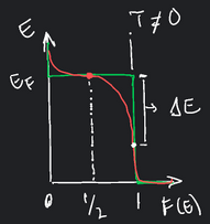
Pointing out a few details, first, if energy level \(E\) is completely occupied by electrons, then the exponential term becomes \(e^{0} = 1\) and \(F_{E} = 1\). Second, for \(E=0\), or an empty energy level, then we have \(F(E) = 0\). Third, for \(T \neq 0\), the curve is broadened slightly as shown in the figure below. Note that the decrease in \(F(E)\) for increasing \(E\) is overemphasized. In practice, the \(\Delta E\) amounts to \(1\%\) of \(E_{F}\).
Combining the density of state in the equation for \(N(E)\) yields,
\[N(E) = \frac{V}{2\pi^{2}} \bigg( \frac{2m}{\hbar^{2}} \bigg)^{3/2} E^{1/2} \frac{1}{\exp \bigg( \frac{E- E_{F}}{k_{B} T} + 1 \bigg)}\]Again, following the cases in the paragraph describing \(F(E)\), \(N(E) = 2 Z(E)\) when \(T \rightarrow 0\) and \(E<E_{F}\), since \(F(E) = 1\). For the case of \(T \neq 0\) and the energy is near the Fermi energy, \(E_{F}\), we can see that \(N(E)\) is broadened as a result,

For electrons in a crystal, the Fermi energy, \(E_{F}\), is the maximum energy electrons occupy at \(T = 0 K\). An expression for \(E_{F}\) can be obtain by defining \(d N^{*}\) between an energy interval \(E\) and \(E+dE\). For the scenerio of obtaining the Fermi energy, the integration is set up for the case \(F(E)=1\) (that is, \(T\rightarrow 0\) and \(E<E_{F}\)) and integrating for \(N^{*}\), the number of elections with an energy equal to or smaller than \(E_{n}\)
\[N^{*} = \int_{0}^{E_F} N(E) dE = \int_{0}^{E_{F}} \frac{V}{2\pi^{2}} \bigg( \frac{2m}{\hbar^{2}} \bigg)^{3/2} E^{1/2} dE\] \[N^{*} = \frac{V}{3\pi^{2}} \bigg( \frac{2m}{\hbar^{2}} \bigg)^{3/2} E^{3/2}\]and solving for \(E_{F}\) in terms of \(N^{*}/V\), the number of electrons per unit volume,
\[E_{F} = \bigg( 3 \pi^{2} \frac{N^{*}}{V} \bigg)^{2/3} \frac{\hbar^{2}}{2m}\]Note that if we consider the case \(T \neq 0\), we can obtain the same expression for \(E_{F}\). Qualitatively, an increase in temperature does not change the number of electrons.
Band Gaps or energy gaps (usually denoted \(E_{g}\)) are the regions where no electronic states can exist as a result of Bloch’s theorem and allowed solutions/energies in a periodic potential.
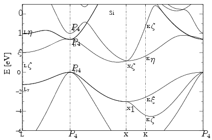 Above is the band diagram of silicon. Notice the band gap energy of about \(1eV\)
Flat band diagrams provide a better way of visualizing band gaps.
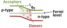 Here is a flat band diagram of a p-n junction.
Above \(E_{g}\) is the conduction band, and below is the valence band. Both of these bands exist near the Fermi level (\(E_{f}\) or \(\mu\)) , is the top most energy of the occupied states
For reference, below is a table of Energy/Band gaps of common materials:
\[\begin{array} {|r|r|}\hline Si & 1.17 eV \\ \hline Ge & 0.74 eV \\ \hline Sn & 0.08 eV \\ \hline C & 5.48 eV \\ \hline \end{array}\]In the presence of an electric field, \(\vec{E}\), electrons in near the Fermi energy (\(E_F\)) experience a force \(F_{external} = e \vec{E}\). Newton’s second law of motion suggests that the acceleration is \(a = F_{external}/m_{e}\). However, in condensed matter, internal forces on the electrons need to be considered due to the interations with other fermionic (or identical) particles in a periodic lattice. Usually written as a fraction of \(m_{e}\), the, the effective mass is denoted as \(m^{*}\) is a “quasi-mass” so-to-speak used to reconcile the electron’s distinct motion (relative to vacuum motion) in a material.
Consider the following parabolic \(E(k)\) band diagram below:
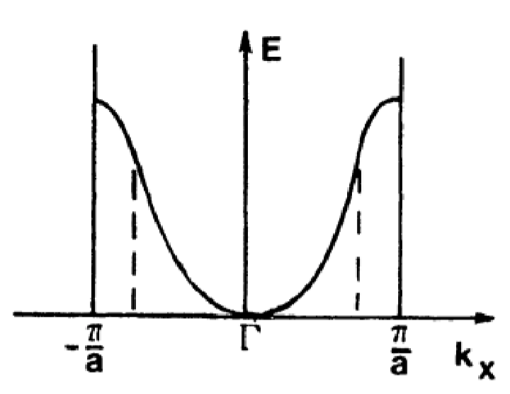
Suppose an electron is subject to a force exerted by an \(\vec{E}\) field. The group velocity is:
\[v_{g} = \frac{d\omega}{dk}\]which is the first derivative of with respect to wavevector \(k\) and plotted below:
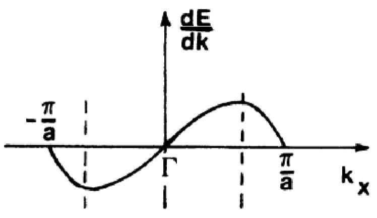
Recalling some wave theory terms; the center frequency is \(\omega = 2\pi\nu\), the wavevector is \(k = \frac{2\pi}{\lambda}\), and \(E=h \nu\), the group velocity can be rewritten as:
\[v_{g} = \frac{d (2\pi\nu)}{dk} = \frac{2\pi(E/h)}{dk} = \frac{1}{\hbar} \frac{dE}{dk}\]Following, the acceleration is simply the time derivative of \(v_{g}\) (don’t forget that this is an implicit derivative!!!):
\[a = \frac{d v_{g}}{dt} = \frac{1}{\hbar^{2}} \frac{d^{2} E}{dk^{2}} \frac{dk}{dt}\]We want to expand on the \(\frac{dk}{dt}\) term into something more useful. Beginning with the wave momentum or the deBrogile momentum:
\[p = \hbar k\] \[\frac{dp}{dt} = \hbar \frac{dk}{dt}\] \[\frac{1}{\hbar} \frac{dp}{dt} = \frac{dk}{dt}\]Coming back to the acceleration equation:
\[a = \frac{1}{\hbar^{2}} \frac{d^{2}E}{dk^{2}} \frac{dp}{dt}\] \[= \frac{1}{\hbar^{2}} \frac{d^{2} E}{dk^{2}} \frac{d(m\vec{v})}{dt}\] \[= \frac{1}{\hbar^{2}} \frac{d^{2} E}{dk^{2}} F\]Following from the familiar \(F=ma\), the effective mass can be expressed as:
\[m^{*} = \hbar^{2} \bigg(\frac{d^{2}E}{dk^{2}} \bigg)^{-1}\]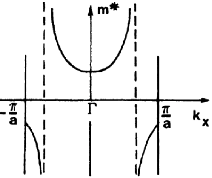
Looking back at the \(E(k)\) diagram reveals that the effective mass, \(m^{*}\) represents the curvature of the band diagram. Note that near Brillouin zone centers, \(m^{*}\) is positive and small, increasing for larger values of \(k\).
As stated at the beginning of this section, these internal forces can be treated as scattering within a lattice which affect the mobility of an electron. Much like the \(F=ma\) result derived earlier, the electron’s effective mass is inversely proportional to it’s mobility. Written in terms of scattering time and effective mass,
\[\mu = \frac{e \tau_{s}}{m^{*}}\]When atomic lattices are subject to vibrations (i.e. thermal energy), the coupled motion can be well represented by a quantum harmonic oscillator. To quickly recap some important features of quantum harmonic oscillator, the Schrodinger takes the form:
\[\frac{\partial^{2} \psi}{\partial x^{2}} + \frac{2M}{\hbar^{2}} \bigg( E - \frac{1}{2} \beta x^{2} \bigg)\]where the spring potential, and its constant \(\beta\), is
\[V(x) = \frac{1}{2} \beta x^{2}\]Of course, the important solution the the Schrodinger equation yields quantized energies equally seperated by \(\hbar \omega\), \(E_{n}\):
\[E_{n} = \bigg( n + \frac{1}{2} \bigg) \hbar \omega\]The coupled vibrations in a lattice can be represented by a \(1-D\) lattice of \(N\) atoms with interatomic spacing \(a\). This string of atoms are subject to longitudinal and transveral modes of oscillation, displaced a distance \(u_{r}\). Wave mechanics tells us that a traveling wave along \(x\) is,
\[u_{r} = A e^{i(kx_{r} - \omega t)}\]where \(k\) is the wavevector and \(A\) is the amplitude. These excitations in the lattice can be represented by a quasi-particle, a phonon. Due to its wave characteristics, several quantities such as energy, momentum, and wavelength are convieniently familiar to its electromagnetic analog, the photon.
Phonon wavelength: \(\Lambda = \frac{2\pi}{k}\)
Phonon Energy: \(E_{ph} = \hbar \omega = h \nu\)
Phonon Momentum: \(p_{ph} = \hbar k\)
Solving for the frequency of vibrations, \(\omega\), one can derive the phonon dispersion relation:
\[\omega = 2 \sqrt{\frac{\beta}{M}} \bigg| \sin{ \frac{1}{2} ka } \bigg|\]where \(\beta\) is the familiar spring constant for a harmonic oscillator and \(M\) is the mass. The maximum frequency, otherwise known as the lattice cut-off frequency is:
\[\omega_{max} = 2 \sqrt{\frac{\beta}{M}}\]Taking the derivative with respect to the wave vector gives the group velocity:
\[v_{g} = \frac{d \omega}{d k} = \sqrt{ \frac{\beta}{M}} a \cos\bigg( \frac{1}{2} ka \bigg)\]Heat capacity is generally defined as the amount of heat a system must gain to raise its temperature by a certain interval. Dimensionally, heat capacity can be written in units of \(J g^{-1} K^{-1}\). However, there are several other denominations of heat capacity in terms of molar mass or when a system is held at constant volume (\(C_{V}\)) and constant pressure (\(C_{P}\)).
Let’s consider a classical atomistic system that is capable of absorbing thermal energy. Such a system can be treated as a harmonic oscillator where the average energy of each oscillator is proportional to the temperature by a factor of \(k_{B}\),
\[E = 3k_{B}T\]where the factor of 3 describes a three-dimensional oscillator. Recall from the kinetic theory of gases (\(PV=nRT\)) that in a closed volume, the kinetic energy of a particle is
\[E_{Kinetic} = \frac{3}{2} k_{B}T\]Similarly, the potential energy also has a similar value, so the total energy of the system picks up a factor of 2:
\[E_{tot} = 2 \cdot \frac{3}{2} k_{B}T\]Applying this to a molar system, the total internal energy per mole is:
\[E = 3 N_{0} k_{B}T\]Taking the derivative with respect to temperature gives the heat capacity. Remember that this was originally derived for a system held at constant volume using the kinetic theory of gases:
\[C_{V} = \bigg( \frac{\partial E}{\partial T} \bigg)_{V} = 3 N_{0} k_{B}\]This is in agreement with experiments when a system is taken to high temperatures. In most solids, as \(T\) grows, \(C_{V}\) approaches the Dulong-Petit value:
\[C_{V}= 3 R = 25 [J mol^{-1} K^{-1}]\]where \(R = N_{A} K_{B}\).
In this section, we consider the effects of free electron contributions to the heat capacity. It is understood that only free electrons with kinetic energies that lie in within \(k_{B}T\) of the Fermi energy (\(E_{F}\)) participate in conductivity. Graphically, this is population of electrons that can be excited in sufficient numbers is represented as the shaded region in the plot below as \(dN\):
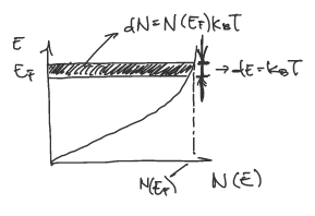
The thermal energy of this population is then:
\[E_{kinetic} = \frac{3}{2} k_{B}T dN\]where \(dN\) can be rewritten as,
\[E_{kinetic} = \frac{3}{2} k_{B}T [ N(E_{F}) k_{B}T]\]The derivative with respect to \(T\) gives:
\[C_{V}^{e} = \bigg( \frac{\partial E}{\partial T} \bigg)_{V} = 3 k_{B}^{2} T N(E_{F})\]An expression for \(N(E_{F})\) can be obtained by combining the density of states, \(g(E_{F})\), with the Fermi distribution \(F(E_{F})\) for case \(E<E_{F}\).
\[N(E_{F}) = \frac{3N^{*}}{2 E_{F}}\]where \(N^{*}\) is the number of electrons with an energy equal to or smaller than \(E_{F}\).
As it stands, without further considerations, \(C_{V}\) is approximately:
\[C_{V}^{e} = \frac{9}{2} \frac{N^{*} k_{B}^{2} T }{ E_{F}}\]However, applying Pauli’s exclusion principle modifies the expression slightly:
\[C_{V}^{e} = \frac{\pi^{2}}{2} \frac{N^{*} k_{B}^{2} T }{ E_{F}} = \frac{\pi^{2}}{2} \frac{N^{*} k_{B} T }{T_{F}}\]Consider an electrically neutral silicon semiconductor.
Intrinsic semiconductors are pure-element semiconducting materials. The number of excited electrons and holes are equal, \(p=n\) such that the product of the electron concentration \(n\) and the number of holes \(p\) gives what’s known as the intrinsic carrier concentration:
\[np=n_{i}^{2}\]The terms \(n\) and \(p\) for electron and hole concentrations can be readily derived using the density of states in a semiconductor.
The density of states for a free electron \(E(k)\) diagram is:
\[g(E) = 2 \frac{d N(E)}{dE} = \frac{1}{2\pi^{2}} \bigg( \frac{2m_{e}}{\hbar^{2}} \bigg)^{3/2} E^{1/2}\]In the case of semiconductors, a similar expression can be written for the density of states of the conduction and valence bands.
\[g(E)_{conduction} = \frac{1}{2\pi^{2}} \bigg( \frac{2 m_{n}^{*}}{ \hbar^{2}} \bigg)^{3/2} ( E - E_{C} )^{1/2}\] \[g(E)_{valence} = \frac{1}{2\pi^{2}} \bigg( \frac{2 m_{p}^{*}}{ \hbar^{2}} \bigg)^{3/2} ( E_{v} - E )^{1/2}\]We can integrate the density of states with the Fermi distribution by using the range of energies (from bottom to top) within the band, to obtain the concentration of \(n\) or \(p\). For example, in the case of the conduction band:
\[n = \int_{E_{C}^{bot}}^{E_{C}^{top}} g(E)_{CB} f(E,T) dE\]It should be mentioned that the probability of occupation of holes will be modified slightly, since it is the absence of electrons
\[p = \int_{E_{V}^{bot}}^{E_{V}^{top}} g(E)_{VB}[1 - f(E,T)] dE\]That being said, there is one more approximation to apply to the Fermi distribution term, \(F(E,T)\). That is, for band gap energies much greater than \(k_{B}T\) at \(300 K\), we can apply the Boltzmann approximation \((E_{G} \gg k_{B}T_{300K})\),
\[F(E,T) = \frac{1}{\exp(\frac{E - E_{F}}{ k_{B}T }) + 1} \approx e^{\frac{E-E_{F}}{ k_{B}T }}\]Applying this approximiation also changes the bounds of integration to infinity. Thus, the full integration for \(n\) and \(p\) concentrations yields:
\[n = N_{C} e^{-\frac{E_{C} - E_{F}}{k_{B}T}}\] \[p = N_{V} e^{-\frac{E_{F} - E_{V}}{k_{B}T}}\]Graphically, this treatment of carrier concentration is plotted below with \(F(E)\) as a function of \(E\):

Two terms that can be expanded upon are \(N_{C}\) and \(N_{V}\), which are also known as the effective density of states. Written in terms of the effective masses of the charge carriers:
\[N_{C} = 2 \bigg( \frac{m_{n}^{*} k_{B}T}{2\pi \hbar^{2}} \bigg)^{3/2}\] \[N_{V} = 2 \bigg( \frac{m_{p}^{*} k_{B}T}{2\pi \hbar^{2}} \bigg)^{3/2}\]Combining all this yields an expression for the intrinsic carrier concentration:
\[n_{i}^{2} = np = N_{C} N_{V} e^{-\frac{E_{g}}{k_{B}T}}\] \[n_{i} = \sqrt{ N_{V} N_{C} } e^{-\frac{E_{g}}{2k_{B}T}}\]In the context of intrinsic undoped semiconductors, excited electrons and holes are created in pairs,
\[n=p=n_{i}\]The intrinsic conductivity of a semiconductor can be written as the sum of the conductivities for each respective charge carrier:
\[\sigma = n q \mu_{n} + p q \mu_{p}\] \[\sigma = n_{i} q (\mu_{n} + \mu_{p})\]Applying an external voltage to the material will make some electrons jump the band gap, supporting charge flow. For example, pure silicon is a group \(IV\) intrinsic semiconductor. The figure below on the left shows the four valence electrons with covalent bonds around each silicon atom.
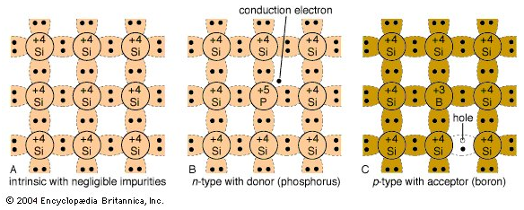
However, as stated earlier, doping semiconductors can dramatically affect the conductivity of the material, making these materials into extrinsic semiconductors. Suppose a group \(V\) atom was introduced into the silicon lattice as shown in the center figure. There will be an free electron (conduction electron) making this impurity a donor. Moreover, since a negatively charged electron was introduced, this make the doped material an n-type semiconductor.
On the other hand, doping the silicon semiconductor with a group \(III\) atom makes the hole a majority carrier and the electrons a minority carrier. The holes accept the free elecron, so the impurity in this case is called an acceptor. Holes are “positively” charged which making this a p-type semiconductor.
Without complexity, doping a material will shift the Fermi energy, \(E_{F}\), towards the valance band or the conduction band depending the dopant charge carrier. For now, the suppose the Fermi energy is a state of “equilibrium” within a band structure.
If the dopant donates electrons making the intrinsic material n-type. The Fermi level in the band gap moves towards the conduction band.
On the other hand, for a p-type material, the Fermi level moves towards the valence band.
Recall the binding energy of an electron in a Hydrogen atom:
\[E_{b} = - E_{1} = \frac{m_{e} e^{4}}{8 \epsilon_{o}^{2} h^{2}} = 13.6 eV\]If we dope, let’s say Silicon with a pentavalent element (\(As^{+}\)), we will need to consider the \(As^{+}\) site along with it’s relative permativity \(\epsilon_{r}\), such that the overall permativity term is, \(\epsilon_{r} \epsilon_{0}\). The effective mass of the electorn in the Si crystal needs to be accounted for as well. All together, the binding energy is then:
\[E_{b}^{Si} = \frac{m_{e} e^{4}}{8 \epsilon_{r}^{2} \epsilon_{o}^{2} h^{2}} = 13.6 eV \bigg( \frac{m_{e}^{*}}{m_{e}} \bigg) \bigg( \frac{1}{\epsilon_{r}^{2} } \bigg)\]Following the discussion from intrinsic semiconductors to maintain the intrinsic carrier concentration,
\[np=n_{i}^{2}\]Donating an electron places a donor energy, \(E_{D}\), close to the conduction band, \(E_{CB}\) assuming that the donor concentration is much greater than intrinsic carrier concentration,
\[N_{D} \gg n_{i}\]the hole concentration can then be written as:
\[p = \frac{n_{i}^{2}}{N_{D}}\]So then the conductivity of the n-type doped semiconducting material is:
\[\sigma = e N_{d} \mu_{e} + e \bigg( \frac{n_{i}^{2} }{ N_{d}} \bigg) \mu_{h} \approx e N_{d} \mu_{e}\]At low temperatures, the probability of occupation follows a similiar argument to the Fermi-Dirac distribution, with a slight modification. Note that once a donor site has been occupied by an electron with a particular spin, no other electrons can take the site, hence a factor of \(1/2\) is multiplied in front of the exponential term to account for this.
\[f_{d} (E_{d}) = \frac{1}{1 + \frac{1}{2} \exp{\bigg( \frac{E_{d}- E_{f}}{kT} \bigg)}}\]There are two classifications of band gaps; direct and indirect. Direct band gaps indicate that momemtum is conserved. In detail, the crystal momentum of electrons and holes are the same in both the conduction and valence band. The band diagram below is of Gallium Arsenide, a direct band gap semiconductor. This is a useful property since the electron can directly emit a photon!
 Notice that the minimal energy state of the conduction band and the maximum energy state of the valence band line up. If plotted in an \(E(k)\) diagram, such as the one for silicon, one would say that these min/max energy states are characterized by a certain crystal momentum (k-vector).
Referring to the band diagram of of Silicon, an indirect band gap semiconductor. Indirect band gaps indiate that some energy was lost in order for momentum to be conserved. The electron must travel pass through an intermediate state in order such that momentum is transferred through the crystal lattice. Graphically, the min-max energies of the Silicon band diagram do not line up.
A table of magnetic properties and their consequences, nicely summarized in Kasap :).

Dimagnetism: Materials that repel or reduces an applied magnetic field, described by a negative magnetic suceptibility. Superconducting materials exhibit “perfect diamagnetism” (\(X_{M} = -1\)) below the Curie temperature (\(T_{C}\)).
Ferromagnetism: Materials that possess large magnetizations even without the presence of an applied field. The magnetic domains of the materials are described as having magnetic order, where all spins are aligned. If the magnetization is lost, a ferromagnetic material can regain its magnetization by placing it in a strong \(\vec{B}\)-field, realigning atomic spins. Upon removal of the strong field, the material maintains most of the magnetization.
For magnetic materials, there is a critical temperature denoted as \(T_{C}\), the Curie temperature or \(T_{N}\), the Neel temperature for which the material loses its magnetic room temperature magnetic properties and becomes paramagnetic, so to speak.
The Curie temperature (\(T_{C}\)) defines the critical temperature above which the material losses its ferromagnetic properties and becomes paramagnetic and above which the material maintains its ferromagnetic properties.
The Neel temperature (\(T_{N}\)) defines the critical temperature Antiferromagnetism:
Paramagnetism:
Ferrimagnetism:
Diffusion describes the thermal transport of atoms as it relates to a concentration gradient. Consider a one dimensional case of diffusion, where unit areas are separated by distance \(a\) with concentrations \(c_1\) and \(c_2\), with atoms diffusion along the \(x\) axis:
\[c_1 = c_2 + a \frac{dc}{dx}\]The net flux of atoms is,
\[\delta n \approx v \delta t a (c_1 - c_2 ) P\]where \(P\) represents the probability of an atom hopping. We arrive at the first law, writing:
\[\frac{\delta n}{\delta t} = j \approx -v a^{2} P \frac{dc}{dx}\]Without needing to elaborate much more, Fick’s Laws of Diffusion in three dimensions are as follows:
Atomic flux is associated with a concentration gradient \(\nabla c\) by:
\[j = -D \nabla c\]where \(D\) is the empirically derived diffusion constant and is temperature dependent.
\[D = D_{0} e^{- E_{v}/k_{B} T}\]The second law describes a “conservation of matter”, requiring that the net flux of atoms should be compensated by an equivalent change in concentration.
\[\frac{dc}{dt} = - \nabla j\]Combining the first and second diffusion laws:
\[\frac{dc}{dt} = \nabla \cdot ( D \nabla c)\]Tensors are a multidimensional objects and can be generalized to contain familiar, lower dimensional vector space quantities. For instance, in order of dimensionality:
Scalar - A tensor of zero rank, specifying a magnitude.
Vector - A tensor of the first rank, specifying magnitude and direction.
9 component matrix (\(m \times m\)) with their own associated pair of axes - A tensor of the second rank.
A tensor’s dimension (\(m\)) describes the number of coordinates needed to describe a position in vector space. The tensor’s rank (\(n\)) provides information about the number of components within the tensor. In the case of 3-D system (\(m^n\) = 9 components).
Consider a 3 component \(\v{a}\) undergoing a transformation \(\v{R}\):
\[\v{a'} = \v{R} \cdot \v{a}\]where \(\v{R}\) is a \(3\times3\) matrix. Written in terms of a linear combination, the transformation can also be written as:
\[\v{a'} = \sum_{j} R_{ij} a_{j}\]with \(j = 1,2,3\).
Scalar products are invariant under rotation (\(\v{a} \cdot \v{b} = \v{a'} \cdot \v{b'}\)). In terms of matrix notation,
\[\vec{a} \cdot \vec{b} = \v{\tilde{a}} \cdot \v{b}\]